Optical STEM: a novel detection technique for fast large-scale single- and multi-beam scanning electron microscopy
- Abstract number
- 51
- Presentation Form
- Poster
- Corresponding Email
- [email protected]
- Session
- Poster Session 1
- Authors
- Arent Kievits (1), Job Fermie (2), Ryan Lane (1), Jacob Hoogenboom (1)
- Affiliations
-
1. Delft University of Technology
2. Delmic B.V.
- Keywords
Optical STEM, multibeam scanning electron microscopy, large-scale electron microscopy
- Abstract text
We demonstrate here a benchmarking study for optical STEM, a new method for scanning electron microscopy. This method could potentially reduce acquisition times as well as outperform imaging with other existing detection modes in specific conditions.
Recent developments in electron microscopy have led to a significant scale-up in the imaging of biological tissues, making throughput a major bottleneck for further progress. Optimization of detection conditions can lead to an up to 20-fold increase in imaging speed for existing detectors (1). New techniques such as multibeam scanning electron microscopy (MB-SEM) (2, 3), where the sample is scanned in parallel by an array of beams, can even provide acquisition speeds that are orders of magnitude larger than for single-beam scanning electron microscopes. Optical scanning transmission electron microscopy (Optical STEM) is a novel detection method that can be applied in both single- and multi-beam electron microscopes and that holds profit to further increase acquisition speeds. We have carried out a detailed characterization, optimization, and benchmarking of Optical STEM detection to quantify its performance in relation to other electron detection techniques. This is particularly important as optical STEM is implemented as a detection method in MB-SEM, but it can also serve as an alternative for regular BSE detection or for a seamless imaging alternative to STEM.
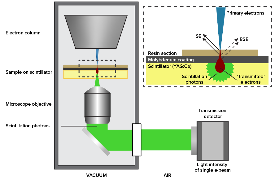
In Optical STEM, ultrathin sections are directly mounted on a cerium-activated yttrium aluminum garnet (YAG:Ce) scintillator coated with a thin layer of molybdenum. This allows for efficient conversion of the transmitted electron signal to a photon signal (Figure 1) which is captured by a high NA objective and projected on a multipixel photon detector (Hamamatsu). We have conducted measurements on rat pancreas tissue stained with reduced osmium and zebrafish larva stained en bloc with reduced osmium followed by en bloc stain or post-stain with neodymium acetate, an alternative for uranyl acetate (4).
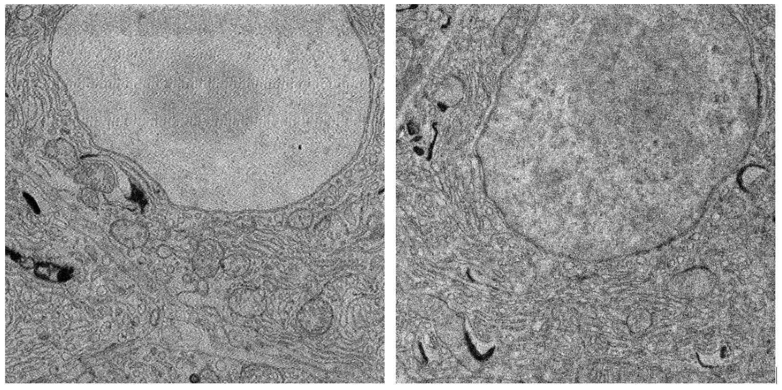
Our work builds on the results from Zuidema & Kruit, 2020 (5), where a model was created to predict the quality of optical STEM images with varying imaging conditions and sample preparation parameters. We have further analysed the performance of optical STEM detection on biological tissue in detail as a function of experimental parameters and benchmarked this against regular BSE detection and conventional STEM. Qualitatively, Optical STEM detection gives EM images with similar contrast and signal (Figure 2). Moreover, we compared quantitative image features such as the spectral signal-to-noise ratio and resolution between the different detection methods. Besides, we discuss the conditions in which optical STEM may outperform other techniques in terms of acquisition speed and show the application in fast large-scale imaging and multi-beam SEM.
In short, we have in detail characterized and optimized a novel detection method for scanning electron microscopy, optical STEM, as an alternative to conventional back scatter electron imaging of ultrathin biological tissue sections. Optical STEM was originally developed as a detection method in multibeam electron microscopy, but can potentially also reduce acquisition times in single beam scanning electron microscopy, outperforming BSE/STEM imaging in specific conditions.
Figure 1: Schematic drawing of setup. The primary beam hits the sample which is on top of the scintillator. The electron signal is converted to a photon signal. A high NA objective is used to capture a large fraction of the signal photons. The detector (a Hamamatsu multipixel photon counter) is located outside of the vacuum.
Figure 2: Comparison of backscatter and transmitted electron detection. (Left) Backscatter detector, 2kV landing energy, 400 pA beam current. (Right) Transmission detector, 5kV landing energy, 400 pA beam current. Sample: rat pancreas tissue (courtesy of Ben Giepmans group, UMC Groningen).
- References
1. R. Lane et al., Optimization of negative stage bias potential for faster imaging in large-scale electron microscopy. J Struct Biol X 5, 100046 (2021).
2. A. Eberle et al., High‐resolution, high‐throughput imaging with a multibeam scanning electron microscope. Journal of microscopy 259, 114-120 (2015).
3. Y. Ren, P. Kruit, Transmission electron imaging in the Delft multibeam scanning electron microscope 1. Journal of Vacuum Science & Technology B, Nanotechnology and Microelectronics: Materials, Processing, Measurement, and Phenomena 34, 06KF02 (2016).
4. J. Kuipers, B. N. G. Giepmans, Neodymium as an alternative contrast for uranium in electron microscopy. Histochem Cell Biol 153, 271-277 (2020).
5. W. Zuidema, P. Kruit, Transmission imaging on a scintillator in a scanning electron microscope. Ultramicroscopy 218, 113055 (2020).